- 您现在的位置:买卖IC网 > Sheet目录362800 > EVAL-AD421EB (Analog Devices, Inc.) Loop-Powered 4 mA to 20 mA DAC
AD421
–3–
REV. C
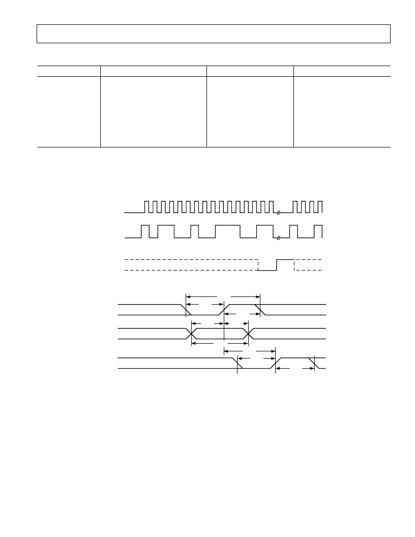
TIMING CHARACTERISTICS
1, 2, 3
Parameter
(B Versions)
Units
Conditions/Comments
t
CK
t
CL
t
CH
t
DW
t
DS
t
DH
t
LD
t
LL
t
LH
100
50
50
30
30
0
50
50
50
ns min
ns min
ns min
ns min
ns min
ns min
ns min
ns min
ns min
Data Clock Period
Data Clock Low Time
Data Clock High Time
Data Stable Width
Data Setup Time
Data Hold Time
Latch Delay Time
Latch Low Time
Latch High Time
NOTES
1
Guaranteed by characterization at initial product release, not production tested.
2
See Figures 1 and 2.
3
All input signals are specified with tr = tf = 5 ns (10% to 90% of V
CC
) and timed from a voltage level of (V
IN
+ V
IL
)/2; tr and tf should not exceed 1
μ
s on any digital
input.
Specifications subject to change without notice.
WORD "N"
WORD "N +1"
1
0
1
1
1
1
1
1
1
1
0
0
0
0
0
0
1
0
0
1
CLOCK
DATA
LATCH
B
(
B
B
B
B
B
B
B
B
B
B
B
B
B
B
B
B
B
B
B
(
Figure 1. Serial Interface Waveforms (Normal Data Load)
CLOCK
DATA
LATCH
t
CK
t
CL
t
CH
t
DS
t
DH
t
DW
t
LD
t
LL
t
LH
Figure 2. Serial Interface Timing Diagram
(V
CC
= +3 V to +5 V, T
A
= T
MIN
to T
MAX
unless otherwise noted)
发布紧急采购,3分钟左右您将得到回复。
相关PDF资料
Eval-AD5025EBZ
Fully Accurate 12-/14-/16-Bit VOUT DAC SPI Interface 2.7 V to 5.5 V in a TSSOP
Eval-AD5045EBZ
Fully Accurate 12-/14-/16-Bit VOUT DAC SPI Interface 2.7 V to 5.5 V in a TSSOP
Eval-AD5065EBZ
Fully Accurate 12-/14-/16-Bit VOUT DAC SPI Interface 2.7 V to 5.5 V in a TSSOP
EVAL-AD5066EBZ
Fully Accurate 16-Bit UnBuffered VOUT DAC SPI Interface 2.7 V to 5.5 V in a TSSOP
EVAL-AD5379EB
40-Channel, 14-Bit, Parallel and Serial Input, Bipolar Voltage-Output DAC
EVAL-AD5381EB
40-Channel, 3 V/5 V, Single-Supply, 12-Bit, Voltage Output DAC
EVAL-AD5382EB
32-Channel, 3 V/5 V, Single-Supply, 14-Bit, Voltage Output DAC
EVAL-AD5383EB
32-Channel, 3 V/5 V, Single-Supply, 12-Bit, Voltage Output DAC
相关代理商/技术参数
EVAL-AD5025EBZ
制造商:AD 制造商全称:Analog Devices 功能描述:Fully Accurate 12-/14-/16-Bit VOUT DAC SPI Interface 2.7 V to 5.5 V in a TSSOP
EVAL-AD5045EBZ
制造商:AD 制造商全称:Analog Devices 功能描述:Fully Accurate 12-/14-/16-Bit VOUT DAC SPI Interface 2.7 V to 5.5 V in a TSSOP
EVAL-AD5060EB
制造商:Analog Devices 功能描述:EVAL BD FOR AD506X DAC 14-/16BIT, SERL INPUT - Bulk
EVAL-AD5060EBZ
功能描述:BOARD EVAL FOR AD5060 RoHS:是 类别:编程器,开发系统 >> 评估板 - 数模转换器 (DAC) 系列:nanoDAC™ 产品培训模块:Lead (SnPb) Finish for COTS
Obsolescence Mitigation Program 标准包装:1 系列:- DAC 的数量:4 位数:12 采样率(每秒):- 数据接口:串行,SPI? 设置时间:3µs DAC 型:电流/电压 工作温度:-40°C ~ 85°C 已供物品:板 已用 IC / 零件:MAX5581
EVAL-AD5061EBZ
功能描述:BOARD EVALUATION AD5061 RoHS:是 类别:编程器,开发系统 >> 评估板 - 数模转换器 (DAC) 系列:nanoDAC™ 产品培训模块:Lead (SnPb) Finish for COTS
Obsolescence Mitigation Program 标准包装:1 系列:- DAC 的数量:4 位数:12 采样率(每秒):- 数据接口:串行,SPI? 设置时间:3µs DAC 型:电流/电压 工作温度:-40°C ~ 85°C 已供物品:板 已用 IC / 零件:MAX5581
EVAL-AD5062EB
制造商:Analog Devices 功能描述:EVAL BD FOR AD506X DAC 14-/16BIT, SERL INPUT - Bulk
EVAL-AD5062EBZ
功能描述:BOARD EVAL FOR AD5062 RoHS:是 类别:编程器,开发系统 >> 评估板 - 数模转换器 (DAC) 系列:nanoDAC™ 产品培训模块:Lead (SnPb) Finish for COTS
Obsolescence Mitigation Program 标准包装:1 系列:- DAC 的数量:4 位数:12 采样率(每秒):- 数据接口:串行,SPI? 设置时间:3µs DAC 型:电流/电压 工作温度:-40°C ~ 85°C 已供物品:板 已用 IC / 零件:MAX5581
EVAL-AD5063EB
制造商:Analog Devices 功能描述:Evaluation Board For 14-/16-Bit, Serial Input, Vout NanoDACs 制造商:Analog Devices 功能描述:EVAL BD FOR AD506X DAC 14-/16BIT, SERL INPUT - Bulk